120V Half-bridge Gate Driver

NSD1224x is a powerful 120V half-bridge gate driver. With peak source/sink current of 3A/-4A and low Rdson of inside ON/OFF MOSFET, it can drive high-power MOSFETs with very low switching losses. The NSD1224x input pin and SW pin can withstand large negative voltage to improve system reliability. The input interlock function prevents the short-through from high-side and low-side MOSFETs in bridge topologies The undervoltage locking (UVLO) is available in both the high-side and low-side drivers. The small communication delay and channel to channel delay matching provide more dead time design margin, further improve efficiency. NSD1224x integrates a built-in bootstrap diode, requiring no external separate diode to save layout space and reduce system costs.
Product Features
- Withstand voltage of VDD power of 20V
- Withstand voltage at SW bridge arm midpoint of -10V to 115V
- Negative withstand voltage of input pin of -10V
- The HS voltage ramp up rate of 50V/ns
- Peak source/sink current 3A/-4A
- Compatible with CMOS/TTL level input
- Input interlock
- Independent UVLO protection for high-side and low-side output
- Integrated high-voltage bootstrap diode
- Typical input/output delay of 16ns
- Typical transmission delay matching between high and low sides of 1ns
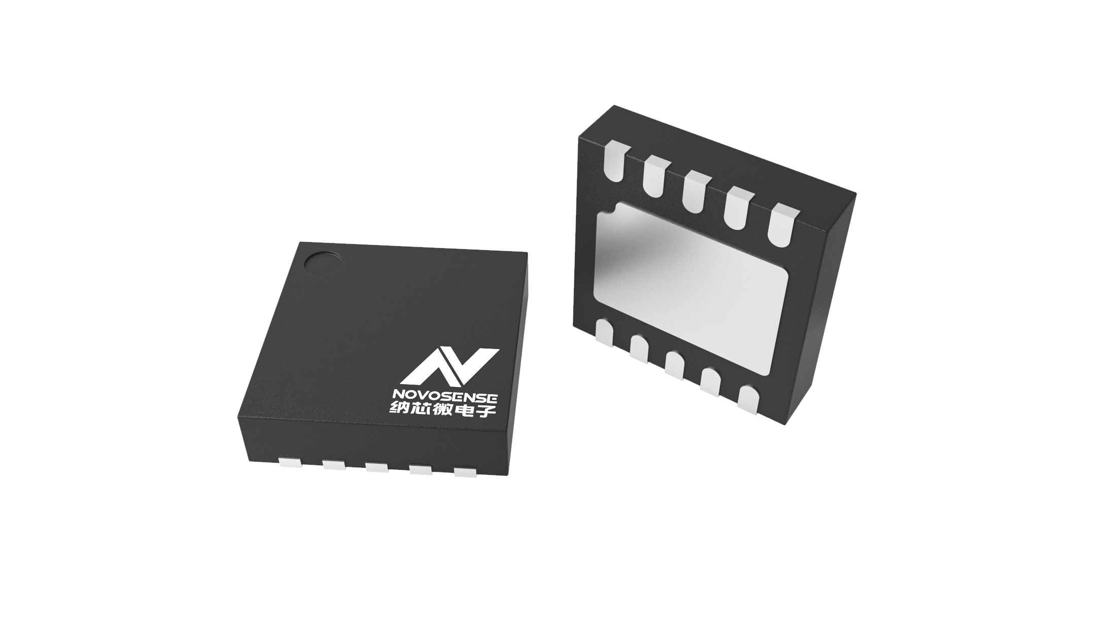
- DFN10 package has enable pin, and the static power consumption is 7μA in standby mode
- Junction temperature range of -40°C to 150°C
Application
- Micro inverter and power optimizer
- Power module
- New energy vehicles

For more product information, please contact us.